Quantum Confinement: Applications, Physics & Strategic Implications
How quantum confinement drives next-gen tech. Explore applications in QLEDs, quantum computing, and strategic implications for 2035.


Quantum Confinement: Fundamental Physics, Engineering Realities, and Strategic Implications for the Next Decade
Summary
Quantum confinement refers to the quantum-mechanical restriction of charge carriers (electrons and holes) within semiconductor nanostructures whose dimensions approach or fall below the material’s exciton Bohr radius. In one, two, or three dimensions, this confinement transforms continuous energy bands into discrete levels, producing size-tunable electronic and optical properties that differ markedly from bulk counterparts. The phenomenon, first predicted theoretically in the 1970s and demonstrated experimentally in the 1980s, now underpins a maturing suite of technologies poised to influence optoelectronics, quantum information science, energy conversion, and biomedical imaging over the coming decade.
Key property changes include a blue-shifted band gap, enhanced exciton binding energy, modified density of states, and increased oscillator strength. These effects enable precise spectral control in quantum-dot light-emitting diodes (QLEDs), single-photon sources for quantum networks, and high-efficiency photovoltaic absorbers. Commercial momentum is accelerating: QLED displays have reached consumer scale, colloidal quantum dots are entering clinical trials for targeted imaging, and spin qubits in silicon quantum dots are demonstrating two-qubit fidelities above 99 percent in laboratory settings.
Strategic implications are threefold. First, quantum confinement offers a scalable pathway to room-temperature quantum devices, potentially compressing the timeline for fault-tolerant quantum computing. Second, supply-chain vulnerabilities; particularly rare-earth and heavy-metal precursors, intersect with geopolitical tensions, necessitating diversified sourcing and recycling strategies. Third, convergence with classical photonics and artificial intelligence could yield hybrid neuromorphic sensors and ultra-secure communication systems. Organizations that invest now in talent pipelines, standards development, and cross-domain integration will capture disproportionate value; those that treat quantum nanomaterials as niche research will risk obsolescence by 2035.
Introduction: From Classical to Quantum Scaling
The semiconductor industry’s relentless pursuit of Moore’s Law has driven feature sizes from micrometers to nanometers, inadvertently crossing the threshold where quantum effects dominate. Early theoretical work by Efros and Efros (1982) and Brus (1984) foresaw that confining carriers in potential wells comparable to the de Broglie wavelength would quantize energy levels. Experimental confirmation arrived in the 1980s with Ekimov et al.’s (1985) glass-embedded semiconductor nanocrystals and Reed et al.’s (1986) etched quantum dots in GaAs.
This “top-down meets bottom-up” inflection point marks the convergence of conventional lithography and colloidal chemistry. Bulk semiconductors exhibit continuous bands and parabolic dispersion; confined systems exhibit atom-like discrete spectra. The transition is not merely academic: it enables engineered band gaps without changing chemical composition, a degree of freedom unavailable to classical materials. Today, quantum confinement sits at the foundation of next-generation technologies that transcend incremental CMOS scaling, promising functional density increases through physics rather than pure geometry.
Core Physical Principles
Quantum confinement arises when at least one spatial dimension of a semiconductor structure is reduced to the order of the exciton Bohr radius (typically 2–20 nm depending on material). Confinement in one dimension yields quantum wells, two dimensions quantum wires (or nanowires), and three dimensions quantum dots.
The simplest model is the particle-in-a-box approximation under the effective-mass framework. The energy levels for a particle in a 3D quantum box are given by:
Enx,ny,nz=8m∗h2(Lx2nx2+Ly2ny2+Lz2nz2)
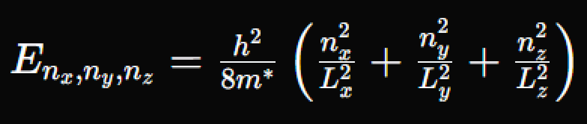
where:
- h is Planck's constant
- m∗ is the effective mass of the particle
- Lx, Ly, and Lz are the confinement lengths in the x, y, and z directions respectively
- nx, ny, and nz are positive integers representing the quantum numbers in each direction
This equation describes the quantized energy states of a particle confined in a three-dimensional rectangular potential well. In real materials, finite barriers and dielectric mismatch modify this picture via the Brus equation, which incorporates Coulomb and polarization terms.
The density of states transforms dramatically: three-dimensional bulk materials show a square-root dependence on energy, while zero-dimensional quantum dots exhibit delta-function-like peaks. This discretization enhances oscillator strength and radiative recombination rates. Strong confinement (structure size << Bohr radius) produces the largest shifts; weak confinement yields subtler corrections. Surface states and dielectric environment further influence binding energies, often increasing exciton stability by factors of 5–10 compared with bulk. These principles have been validated across II-VI, III-V, and group-IV systems.
Observable Effects on Material Properties
The most prominent macroscopic signature is the size-dependent blue-shift of the optical band gap. For CdSe quantum dots, emission can be tuned continuously from 650 nm (bulk-like) to 450 nm as diameter drops from 6 nm to 2 nm. Exciton binding energy rises from ~15 meV in bulk CdSe to >200 meV in strongly confined dots, enabling room-temperature excitonic effects.
Absorption and photoluminescence spectra narrow dramatically, with full-width-at-half-maximum values below 30 nm in monodisperse ensembles. Transport properties shift toward ballistic conduction in nanowires, while quantum dots exhibit Coulomb blockade and single-electron tunneling; foundations for single-electron transistors. A comparison table illustrates typical shifts:
- Bulk GaAs: band gap 1.42 eV, exciton binding 4 meV
- 10 nm quantum well: band gap ~1.55 eV, binding ~12 meV
- 5 nm InGaAs quantum dot: band gap ~1.8 eV, binding >50 meV
Silicon nanowires show phonon confinement effects that alter thermal conductivity by an order of magnitude, critical for thermoelectric applications. These changes are now routinely engineered with sub-nanometer precision.
Fabrication and Scalability Approaches
Two complementary routes exist. Top-down methods, including electron-beam lithography, reactive-ion etching, and atomic layer deposition, offer site-controlled placement compatible with CMOS but suffer from surface damage and limited throughput. Bottom-up approaches include colloidal synthesis (Murray et al., 1993), molecular-beam epitaxy, and vapor-liquid-solid growth, can produce near-perfect crystallinity and narrow size distributions at gram-to-kilogram scales.
Current challenges center on uniformity (σ < 5 % required for displays), defect density (<10¹¹ cm⁻² for qubits), and heterogeneous integration. Recent advances include site-controlled InAs quantum dots via droplet epitaxy and self-assembly on patterned substrates achieving >95 % positional yield. Hybrid processes combining nanoimprint lithography with colloidal deposition are closing the gap toward 300 mm wafer-scale manufacturing. Yield and cost models now project sub-dollar-per-square-centimeter pricing for QLED films by 2028, contingent on precursor recycling.
Commercial and Strategic Applications
Optoelectronics and displays. QLEDs have surpassed OLED efficiency and lifetime in red and green, with Samsung and BOE shipping millions of units. Market consensus projects the quantum-dot display sector to exceed $10 billion by 2028.
Quantum information science. Self-assembled InGaAs dots serve as deterministic single-photon sources with >98 % indistinguishability; silicon quantum dots host spin qubits with coherence times exceeding 100 µs at 1 K. Intel and Quantum Motion pilots demonstrate 50-qubit arrays on 300 mm wafers.
Energy. Quantum-dot sensitized solar cells have reached 18 % lab efficiency; photocatalysis with TiO₂–CdS heterostructures shows promise for CO₂ reduction. Analyst forecasts place the quantum-dot PV market at $2–4 billion by 2030.
Biomedical. Cadmium-free InP and carbon dots enable multiplexed fluorescence imaging and theranostics; Phase II trials for tumor-targeted imaging are underway. Regulatory pathways for heavy-metal-free formulations are maturing.
Sensors and computing. Single-electron transistors operate at room temperature in specialized geometries; neuromorphic synapses using quantum-dot arrays achieve 10⁶ synaptic weights per cm². Each domain carries distinct supply-chain and IP considerations, with export controls already applied to certain III-V quantum nanostructures.
Challenges, Risks, and Policy Considerations
Technical hurdles remain formidable: heavy-metal toxicity in Cd- and Pb-based dots, rapid decoherence at elevated temperatures, and thermal quenching above 100 °C. Environmental, health, and safety frameworks lag; the EU’s REACH restrictions and U.S. TSCA updates are only partially harmonized. Geopolitically, China controls ~70 % of rare-earth processing critical for MBE sources, while U.S. CHIPS Act funding targets domestic quantum-nanofabrication capacity.
Talent shortages are acute; fewer than 5,000 PhD-level researchers globally combine materials synthesis with quantum-device engineering. Standards for quantum-dot metrology and interoperability are absent, slowing adoption. Coordinated public-private investment in open testbeds and workforce programs is essential.
Future Outlook and Strategic Recommendations
By 2030, hybrid quantum-classical photonic chips integrating thousands of confined-spin qubits with CMOS control layers are plausible. Convergence with AI will enable adaptive quantum sensors for edge computing. Room-temperature topological protection or singlet-triplet qubits could disrupt cryogenic requirements. Ten-year horizons include on-chip quantum repeaters and ultra-efficient solid-state lighting consuming <10 % of current display power.
Recommendations:
- Corporations should establish cross-functional “quantum confinement centers of excellence” linking materials, device, and systems teams.
- Governments must fund standardized 300 mm pilot lines and international talent visas.
- Industry consortia should accelerate heavy-metal-free material roadmaps and circular-economy protocols.
Conclusion
Quantum confinement transforms fundamental physics into engineered functionality at scales unattainable by classical means. The next decade will determine whether this capability becomes a strategic differentiator or a missed opportunity. Disciplined investment, responsible innovation, and international collaboration will decide the outcome.
Key Takeaways
- Quantum confinement enables size-tunable properties without compositional change, driving breakthroughs across five major sectors.
- Manufacturing scalability has reached pilot-line maturity, but uniformity and integration remain gating factors.
- Strategic risks center on materials supply chains, talent, and regulatory readiness.
- Convergence with photonics and AI positions quantum nanomaterials as a platform technology for 2030–2035.
- Early movers who treat the field as core infrastructure rather than incremental R&D will secure competitive advantage.