Nanotechnology Infrared Optics for Astronomy Missions
Metalenz, DARPA ENVision, HWO, PRIMA, T2SL detectors, ALD coatings, and China's germanium ban: nanophotonic IR optics for astronomy assessed in full.

Nanotechnology Infrared Optics for Astronomy: Metalenses, Quantum Dots, and Why a Chinese Export Ban Threatens the Next Space Telescope
1. Summary
Nanotechnology-enabled infrared (IR) optics, including metasurface “metalenses,” nanostructured antireflection coatings, plasmonically enhanced detectors, type-II strained layer superlattice (T2SL) and quantum-dot focal-plane arrays, photonic-crystal filter arrays, and atomic-layer-deposited (ALD) protective films, are no longer a frontier laboratory curiosity but a convergent technology stack that is now being procured, qualified, and (in lower-TRL form) infused into NASA, ESA, and Department of War programs. The single most consequential finding of this report is that nanophotonic IR optics are likely to define the cost, schedule, and science return envelope of the next generation of flagship and Probe class astronomy missions, most prominently the Habitable Worlds Observatory (HWO) and the PRobe far-Infrared Mission for Astrophysics (PRIMA), and that U.S. leadership in this domain is materially exposed to two simultaneous bottlenecks: Chinese dominance of the germanium and gallium feedstocks for conventional IR optics, and the constraint that ITAR/EAR controls place on multilateral collaboration in detector and metasurface fabrication [1][2][3][4].
1.1 Bottom-Line Findings
First, evidence from peer-reviewed and government-funded programs indicates that metalens technology has crossed a credibility threshold in 2022–2025. Wafer-scale metalenses with 80 mm and 100 mm apertures have been demonstrated with diffraction limited focusing efficiencies above 80% in the near-IR, manufactured using deep-ultraviolet (DUV) photolithography compatible with mainstream CMOS foundries [5][6]. DARPA’s EXTREME and follow-on ENVision programs, together with the NGA Metalenses program, have explicitly transitioned this technology from basic science to fieldable infrared imaging prototypes [7]. Second, IR detector technology continues to advance along two parallel paths: HgCdTe and Si:As impurity-band-conduction (IBC) arrays, which are the workhorses of the James Webb Space Telescope (JWST), and emerging T2SL and colloidal quantum-dot (CQD) photodetectors offering smaller pixel pitch, higher operating temperatures, and lower fabrication cost [8][9][10]. Third, market and supply-chain conditions are paradoxical: the broader nanophotonics market is on a high-single-digit to mid-teens compound annual growth rate (CAGR) trajectory through 2034, while the upstream feedstock for IR optics (particularly germanium) has become a geopolitically weaponized commodity following Chinese export controls in 2023–2024 [11][12][13][14]

1.2 Strategic Significance
For policymakers, the convergence of astronomy missions and dual-use IR sensing creates both an opportunity and an exposure. The same metasurface-based focal-plane architectures that enable a HWO coronagraph capable of distinguishing an Earth-analog exoplanet at 10⁻¹⁰ contrast are functionally adjacent to architectures used in missile warning, ISR, and persistent surveillance from space [7][15]. For institutional investors, this means the capital structure of the nanophotonics supply chain, fabless designers (e.g., Metalenz, Tunoptix), pure-play foundries (UMC, GlobalFoundries, STMicroelectronics in their photonics roles), and integrated detector manufacturers (Teledyne, Leonardo DRS, II VI/Coherent), is a single technology base with multiple revenue streams across consumer biometrics, defense ISR, and astronomy [16][17]. For research institutions, the bottleneck is no longer demonstrating proof-of-concept devices in the laboratory; it is advancing through the so-called “mid-TRL gap” between TRL 3 and TRL 6 where flight qualification is decided [18].
1. Summary
1.1 Bottom-Line Findings
1.2 Strategic Significance
2. Contextual Background
2.1 Historical Evolution of Infrared Astronomy
2.2 Physics of Infrared Detection and Limits of Conventional Optics
2.3 How Nanotechnology Addresses These Limitations
3. Key Players and Stakeholders
3.1 Government Space Agencies
3.2 Research Institutions and National Laboratories
3.3 Defense-Adjacent Organizations
3.4 Private-Sector Companies
3.5 Standards Bodies
4. Technical and Operational Considerations
4.1 Nanostructured Antireflection Coatings for Broadband IR Transparency
4.2 Metamaterial Flat Optics (Metalenses) for Infrared Wavelengths
4.3 Quantum Dot and Superlattice IR Photodetectors
4.4 Plasmonic Enhancement of IR Detector Sensitivity
4.5 Photonic Crystal Filters for Spectral Selection
4.6 Cryogenic Compatibility and Space-Qualification
4.7 Manufacturing Scalability
4.8 Integration Challenges
4.9 Performance Benchmarks vs. Conventional Optics
5. Economic and Market Dynamics
5.1 Market Size and Growth Trajectory
5.2 Government R&D Funding
5.3 Venture Capital Flows
5.4 Cost Structures for Nano-Fabrication at Space-Qualification Grade
5.5 Commercial Crossover Potential
5.6 Supply Chain Considerations for Rare Materials
6. Regulatory Landscape
6.1 ITAR and EAR Controls on IR Optics
6.2 NASA TRL Requirements
6.3 ESA Qualification Standards
6.4 Spectrum Allocation and Environmental Regulation
6.5 Intellectual Property Considerations
7. Geopolitical and Strategic Dimensions
7.1 Dual-Use Nature of IR Optics
7.2 U.S.–China Competition in Nanophotonics and Space Technology
7.3 Allied Cooperation Frameworks
7.4 Technology Transfer Risks
7.5 Strategic Importance
8. Risk Matrix
9. Strategic Recommendations
9.1 For Policymakers and Government Agencies
9.2 For Institutional Investors and Industry Executives
9.3 For Research Institutions
10. Caveats and Confidence Calibration
11. References
2. Contextual Background
2.1 Historical Evolution of Infrared Astronomy
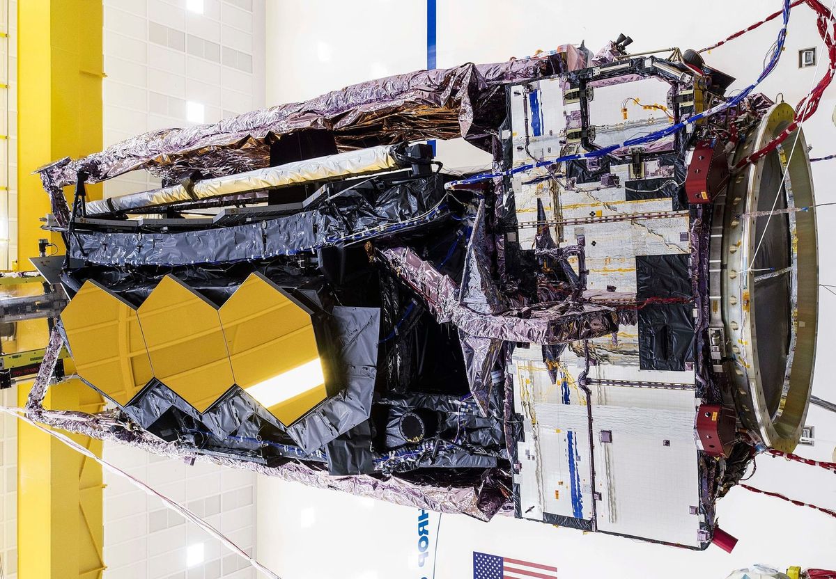
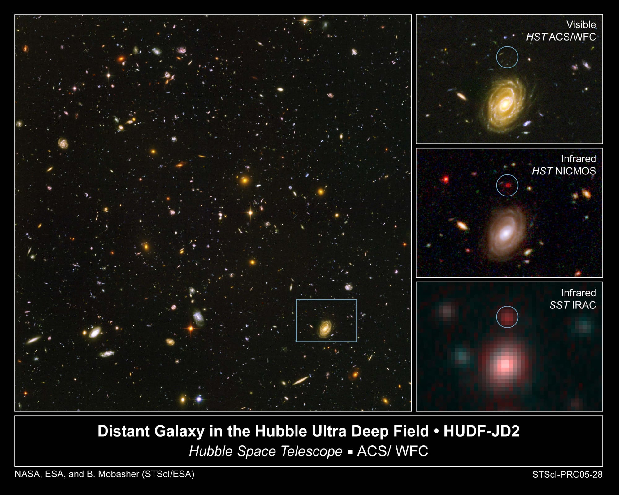
Infrared astronomy from space began as a sortie-mode shuttle concept (the Shuttle Infrared Telescope Facility) proposed at NASA Ames in 1971 and culminated in the Spitzer Space Telescope, launched 25 August 2003 with an 85-cm beryllium primary mirror cooled to 5.5 K and an Earth-trailing solar orbit, operating until January 2020 [19]. Spitzer’s three instruments; the Infrared Array Camera (IRAC), Infrared Spectrograph (IRS), and Multiband Imaging Photometer for Spitzer (MIPS), collectively defined what large-format Si:As IBC and Si:Sb arrays could achieve in cryogenic space [19][20]. The James Webb Space Telescope (JWST), launched in December 2021, represents a generational advance: a 6.5 m segmented gold-coated beryllium primary, passively cooled by a five-layer Kapton sunshield, with a Mid-Infrared Instrument (MIRI) that uses 1024 × 1024 Si:As IBC arrays sensitive from 5 to 28.5 µm and operating below 7 K via active cryocooling, while the near-IR instruments (NIRCam, NIRSpec, NIRISS, FGS) use Teledyne H2RG HgCdTe arrays operating at approximately 37 K [21][22][23][24].
Looking forward, two flagship and Probe-class missions define the 2030s science agenda. The Habitable Worlds Observatory (HWO), recommended by the 2020 National Academies’ decadal survey “Pathways to Discovery in Astronomy and Astrophysics for the 2020s,” is targeted at directly imaging at least 25 potentially habitable exoplanets and characterizing their atmospheres for biosignatures across the ultraviolet, optical, and near infrared bands [25][26]. NASA established a dedicated Technology Maturation Project Office at Goddard Space Flight Center in 2023, and on 5 January 2026 NASA announced the selection of industry proposals (BAE Systems, Lockheed Martin, others) to advance HWO technologies, with picometer-level wavefront stability identified as the binding requirement [25][27]. In parallel, the PRobe far-Infrared Mission for Astrophysics (PRIMA), selected for Phase A in October 2024 and competing with the Advanced X-ray Imaging Satellite (AXIS) for a single 2032 launch slot, would deploy a 1.8-m telescope cryogenically cooled to 4.5 K with two instruments providing imaging and spectroscopy from 24 to 235 µm [28][29].

2.2 Physics of Infrared Detection and Limits of Conventional Optics
Three physical limits constrain conventional refractive and reflective IR optics. First, Fresnel reflection losses at the air–substrate interface for high-index IR materials such as germanium (n ≈ 4.0 at 10 µm) reach roughly 36% per uncoated surface, severely degrading throughput [30]. Second, broadband chromatic dispersion in refractive optics requires multi-element designs that add mass, complexity, and cryogenic stress paths. Third, conventional detectors require active cooling; JWST’s MIRI Si:As arrays operate below 7 K, achievable in space only through a multi-stage closed-cycle cryocooler, which drives spacecraft mass, power, and reliability margins [22][24].
2.3 How Nanotechnology Addresses These Limitations
Nanostructured antireflection (AR) coatings, fabricated by step-graded oblique-angle deposition or self-assembled subwavelength gratings, have demonstrated below 4% reflectance on GaSb in the long-wave IR (LWIR), compared with ~34% for uncoated ADS substrates, while maintaining mechanical integrity under cryogenic and launch-vibration environments [30][31]. Metasurface optics; flat, subwavelength-patterned dielectric or semiconductor structures, replace bulk refractive elements with single-layer designs that can be co-fabricated with detector wafers; recent demonstrations include 80 mm aperture near-IR metalenses with 80.84% peak efficiency at 1450 nm, 100-mm visible all-glass metalenses imaging the Sun and Moon, and centimeter-scale achromatic LWIR metalenses at 8–12 µm [5][6][32]. Plasmonic enhancement integrates subwavelength metallic nanostructures with detector active layers to concentrate optical fields, increasing absorption in thin InSb, HgCdTe, and quantum-dot-in-a-well (DWELL) detectors and enabling spectrally selective response [33][34]. Photonic-crystal filter arrays bonded directly to focal planes enable computational spectroscopy with form factors 5–10 times smaller than conventional grating spectrometers, as proposed for the ESA Scout TANGO concept [35]. Quantum-dot infrared photodetectors (QDIPs), colloidal PbS-based SWIR detectors, and T2SL InAs/GaSb detectors offer smaller pixel pitch (down to 6 µm in HexaBlu MWIR), higher operating temperatures, and pathways to reduce dependence on HgCdTe [9][36]. Atomic layer deposition (ALD) provides sub-nanometer-thickness control for protective and AR coatings, enabling silver-based mirrors with alumina or magnesium fluoride protection layers that have been integrated into NASA Goddard SmallSat astrophysics missions (SPRITE, Aspera) [37][38].
3. Key Players and Stakeholders
3.1 Government Space Agencies
NASA dominates the demand side through the Astrophysics Division (FY2025 enacted at approximately $1.6 billion), with technology maturation routed through the Strategic Astrophysics Technology (SAT) program, the Astrophysics Research and Analysis (APRA) program, and the Habitable Worlds Observatory Great Observatory Maturation Program (GOMAP). SAT was established in 2009 specifically to bridge the TRL 3–6 gap, and a 2021 review found it had executed approximately 100 competed grants advancing detectors, coatings, coronagraphs, and starshades [18][39]. The European Space Agency (ESA) contributes through Voyage 2050, including a UK-led near-IR Integral Field Spectrograph for the HWO coronagraph and the TANGO Scout methane-monitoring mission incorporating photonic-crystal spectrometry [26][35]. JAXA contributes through ISAS infrastructure and historical participation in cryogenic AR coating development for cosmic microwave background (CMB) instruments such as POLARBEAR-2 [31].
3.2 Research Institutions and National Laboratories
The Capasso Lab at Harvard University holds foundational metasurface intellectual property exclusively licensed to Metalenz, Inc., and continues to publish enabling work on holey metalenses, all-glass visible metalenses, and hybrid meta-optics [6][16][40]. The Pennsylvania State University (Ni group, with NASA Goddard collaboration) demonstrated the first wafer-scale near-IR metalens telescope [5]. The Jet Propulsion Laboratory (JPL) Microdevices Laboratory operates the leading U.S. capability in ALD-deposited delta-doped silicon imagers, achieving record UV quantum efficiency from 150–300 nm, and develops solid-immersion metalenses for infrared focal-plane arrays in collaboration with Capasso [37][41]. MIT, the University of Washington (Tunoptix spinout), the University of Texas (Wasserman group), and the University of Massachusetts Amherst contribute to DARPA’s EXTREME and ENVision portfolios [7][17][42]. National laboratories play differentiated roles: Sandia developed the MIRAGE simulation tool for large-scale metalens optimization under the DARPA/NGA programs; the Naval Research Laboratory contributes volumetric 3D metamaterial imaging; and the Air Force Research Laboratory (AFRL) characterizes meta-optics for unmanned aerial system payloads [7].
3.3 Defense-Adjacent Organizations
DARPA’s EXTREME program (initiated 2016) and ENVision program have made the Department of War the largest single funder of metasurface IR optics globally, with explicit transition pathways through the AFRL Strategic Development Planning and Capabilities Office (SDCP) into Integrated Compact EO/IR Systems (ICES), the XQ-58 Valkyrie unmanned combat aerial vehicle, and the Air Launched Off-Board Operations (ALOBO) program [7]. The National Geospatial-Intelligence Agency funded a separate 2018 Metalenses program for unmanned aerial system optics. In-Q-Tel and the Defense Innovation Unit serve as commercialization conduits.
3.4 Private-Sector Companies
The infrared detector industry is structured as a small set of vertically integrated players. Teledyne FLIR/Teledyne Imaging Sensors manufactures the H2RG HgCdTe arrays used across JWST’s near-IR instruments, the Nancy Grace Roman Space Telescope, and most major astronomy missions, and is transitioning portions of its product line to T2SL “high-operating-temperature” (HOT) detectors [8][24]. Leonardo DRS operates a vertically integrated HgCdTe foundry in Dallas and has developed HgCdTe linear-mode electron-initiated avalanche photodiodes that enable NASA space lidar missions [10]. Coherent Corp. (formerly II-VI Incorporated, after the Rofin Sinar and EOT acquisitions) supplies broad photonic components, while Raytheon Technologies (RTX) and BAE Systems integrate at the system level [16][17]. The fabless metasurface segment is led by Metalenz, Inc. (founded 2016, more than 150 patent applications, partnership with STMicroelectronics yielding more than 140 million units shipped in consumer biometrics by 2025, and a UMC 12-inch foundry production agreement) and by Tunoptix (DARPA STTR-funded, University of Washington Nanofabrication Facility) [16][17][43]. Magnolia Optical Technologies leads commercial development of nanostructured AR coatings under NASA Earth Science Technology Office and U.S. Army SBIR contracts [30] [31].
3.5 Standards Bodies
Standards activity is fragmented. The International Organization for Standardization (ISO TC 172 Optics and Photonics), SPIE, Optica (formerly OSA), the European Cooperation for Space Standardization (ECSS, particularly ECSS-Q-ST-70-06C on space materials), and the NIST National Cybersecurity Center of Excellence (NCCoE) for space-domain cybersecurity all set partial frameworks [44].
4. Technical and Operational Considerations
4.1 Nanostructured Antireflection Coatings for Broadband IR Transparency
The state of the art in nanostructured AR for astronomy applications combines step-graded refractive index profiles (achieved by oblique-angle physical vapor deposition or by glancing-angle ALD) with subwavelength gratings. Magnolia Optical’s nanowire-based and step-graded ZnS coatings on GaSb have shown reflectance below 4% across the 8–14 µm LWIR band, with documented stability under cryogenic cycling and launch-equivalent vibration [30][31]. For large-diameter (≥500 mm) cryogenic IR filters used in CMB and far-IR astronomy, two-layer mullite/Skybond foam AR coatings have been qualified for POLARBEAR-2 and ACTpol architectures [31]. The principal limitations are residual scatter from process-induced defects and the difficulty of producing uniform thickness over the large, curved substrates required by future flagship apertures.
4.2 Metamaterial Flat Optics (Metalenses) for Infrared Wavelengths
Three demonstrations between 2022 and 2025 are particularly germane to astronomy. First, the Penn State/NASA Goddard 80-mm aperture near-IR metalens telescope used DUV photolithography with reticle-rotation pattern stitching to leverage radial symmetry, producing diffraction-limited lunar imagery at 1450 nm with 80.84% peak focusing efficiency [5]. Second, the Harvard 100-mm all-glass visible metalens, fabricated using conventional CMOS-compatible processes and comprising 18.7 billion nanostructures, demonstrated imaging of the Sun, Moon, and distant nebulae and survived launch-equivalent vibration testing [6][45]. Third, the National University of Defense Technology (Changsha) demonstrated a 6.36-cm-diameter all-silicon achromatic LWIR metalens operating at 8–12 µm with a normalized focal-length shift below 3.3 × 10⁻⁴ across the band [32]. NASA’s Earth Science Technology Office (ESTO) has separately funded the Metalens Origami Deployable Lidar (MODeL) Telescope concept (Stephen, Goddard) as a SmallSat-deployable architecture [42]. The remaining technical gaps are aperture scaling to the meter class required for flagship telescopes, achromatic broadband performance across an octave or more of wavelength, and validation of long-term radiation induced degradation in the Earth–Sun L2 environment.
4.3 Quantum Dot and Superlattice IR Photodetectors
Three detector classes are competing to displace incumbent HgCdTe and Si:As IBC for next-generation missions. T2SL InAs/GaSb and InAs/InAsSb structures (offered commercially by Teledyne FLIR, Leonardo DRS, and others) provide MWIR/LWIR detection with smaller pixel pitch, higher operating temperatures, and reduced reliance on mercury-bearing semiconductors [8][46]. Quantum-dot-in-a-well (DWELL) detectors integrated with plasmonic resonance layers achieve wavelength controllability and 1/f-noise advantages [34]. Colloidal quantum-dot (CQD) photodetectors based on PbS and HgTe offer solution-processable fabrication, broad spectral tuning across SWIR/MWIR, and low cost; ICFO Barcelona, ISRO, and the Nagoya/Mitsubishi consortium have published patents for up-conversion architectures applicable to space imaging [9] [47]. For astronomy specifically, NASA’s APRA-funded “Noiseless Single Photon Counting Mid-Infrared Detector” project at Goddard targets a first-of-its-kind photon counting architecture [18].
4.4 Plasmonic Enhancement of IR Detector Sensitivity
Plasmonic structures (arrays of subwavelength metallic apertures, nano-antennas, or Fano-resonant metamaterials) concentrate optical fields by factors as large as 10⁵ near the absorber. Demonstrations include plasmonic enhancement of ultrathin InSb absorption for room-temperature MWIR detection, integration with VO₂ nanobeam bolometers (Magnolia/U.S. Army SBIR), and broadband LWIR plasmonic absorbers achieving above 60% absorptance in spintronic Poisson bolometers [33][34][48]. For astronomy, the relevance is twofold: relaxation of cooling requirements (which drives mass and power) and enabling spectrally selective on-pixel filtering.
4.5 Photonic Crystal Filters for Spectral Selection
Photonic-crystal filter arrays bonded directly onto focal planes implement computational spectroscopy via compressive sensing. The ESA TANGO Scout methane-monitoring concept and SRON-led prototypes use 700-nm-thick amorphous-silicon photonic crystals on quartz substrates, achieving methane retrieval errors below 1.0% in instruments 5–10× smaller than conventional grating spectrometers [35]. The astronomy application path runs through hyperspectral imaging instruments such as PRIMA’s PRIMAger (R ~ 8 from 25 to 84 µm) and similar concepts.
4.6 Cryogenic Compatibility and Space-Qualification
Three failure modes dominate cryogenic qualification for nanostructured optics: differential thermal contraction at material interfaces leading to delamination or microcracking; phase change behavior in tunable metasurfaces (e.g., GST-based reconfigurable metalenses) that can become non-functional below operational thresholds; and surface contamination during pre-launch integration that disproportionately affects subwavelength features. JWST’s mirror polishing methodology (measuring cryogenic surface figure error at the X-Ray Calibration Facility and using that to drive final room-temperature polishing to a 17 nm cryo SFE target) illustrates the precision required [21]. Evidence suggests, though direct flight heritage is limited, that all-dielectric Si and SiN metasurfaces can be qualified to similar standards using ALD-deposited protective overcoats.
4.7 Manufacturing Scalability
The decisive economic question is whether nano-fabricated optics can scale at semiconductor-foundry economics. Three pathways are credible. DUV photolithography on 200-mm and 300-mm wafers, demonstrated by Metalenz at UMC and STMicroelectronics, is the current high-volume route, with the trade-off of fixed minimum feature sizes [5][16] [43]. Nanoimprint lithography (NIL) and electron-beam-written master-template approaches, demonstrated under DARPA EXTREME by University of Massachusetts Amherst and Harvard, offer flexibility but lower throughput [40]. ALD and atomic layer etching (ALE), pioneered for space applications at JPL, provide atomic-precision conformal coatings on three-dimensional and curved substrates [37][38]. Self-assembly approaches remain at lower TRL.
4.8 Integration Challenges
Integration with telescope architectures faces three issues. First, the f-number and field-of view of metalenses currently lag refractive optics, particularly for wide-field-imaging instruments. Second, polarization sensitivity of metasurfaces requires careful design and characterization, especially for coronagraph instruments where polarimetric leakage degrades contrast. Third, alignment tolerances for HWO-class missions are at the picometer level, well beyond the demonstrated stability of any current metasurface architecture [27].
4.9 Performance Benchmarks vs. Conventional Optics
A conservative benchmarking exercise based on published peer-reviewed data suggests the following: in throughput, well-designed dielectric metalenses approach 80–90% in narrow bands but typically lose 10–30% across an octave, compared to better than 95% for high quality conventional refractive optics with multilayer AR. In mass and volume, metalenses can reduce optical system mass by factors of 5–10 for comparable apertures below ~10 cm, with the gap narrowing at larger apertures. In radiation hardness, evidence is preliminary; published 2D-material radiation-tolerance studies indicate that gamma, proton, and electron fluxes typical of low Earth orbit can degrade quantum emitters and field-effect transistors but that interface-rich nanostructured materials show some inherent radiation tolerance [49][50].
5. Economic and Market Dynamics
5.1 Market Size and Growth Trajectory
The broader photonics market was estimated at approximately $1.09 trillion in 2025 and is projected to reach $1.48 trillion by 2030 at a 6.3% CAGR by MarketsandMarkets, with the infrared segment representing the largest wavelength category [11]. Independent estimates of the nanophotonics sub-segment vary widely, from $16.0 billion in 2024 (IMARC Group, 6.8% CAGR) to $20.5 billion (Global Market Insights, 16% CAGR), and the dispersion reflects definitional inconsistencies more than disagreement on direction [12][51]. For space-grade IR optics specifically, the market is opaque because much of the demand is government and classified; analysts agree, however, that the IR segment is one of the fastest-growing wavelength categories with reported CAGRs of 9.5% (Precedence Research) [52].
5.2 Government R&D Funding
NASA’s enacted FY2025 budget was approximately $24.8 billion, with the Astrophysics Division at $1.6 billion. The FY2027 President’s Budget Request, released April 2026, proposed a 23% cut to NASA’s overall budget, including a 47% cut to the Science Mission Directorate and a 65% cut to Astrophysics, though Congress has historically rejected the largest proposed cuts [53][54][55]. The Astrophysics Research and Analysis budget has been the primary funding vehicle for low-TRL detector and optics research; the FY2027 request would reduce APRA from $116.7 million (FY2024) to $46.6 million Astrobites [55]. The Department of War provides substantial parallel funding through DARPA EXTREME/ENVision and through the Department of the Air Force’s Strategic Development Planning and Capabilities Office [7]. EU Horizon Europe and ESA technology maturation programs add additional capacity, with national efforts in Germany, France, Italy, and the United Kingdom growing.
5.3 Venture Capital Flows
Defense-tech venture funding totaled approximately $2.5 billion in 2024 by Crunchbase data, with space-tech venture funding nearly reaching $6 billion. Photonics-specific venture activity has been concentrated in silicon photonics for AI data centers (Lightmatter, Lightelligence, CamGraPhIC) and metasurfaces for biometrics and 3D sensing (Metalenz, which closed a $30 million Series B led by Neotribe Ventures in October 2022) [16][56][57]. Direct astronomy-specific venture investment is minimal; most space-grade optical innovation is funded through SBIR/STTR, In-Q-Tel, and corporate venture arms (RTX Ventures, Lockheed Martin Ventures).
5.4 Cost Structures for Nano-Fabrication at Space-Qualification Grade
Published cost data is sparse, but a defensible estimate from triangulating SBIR Phase II awards (typically $1–2 million), DARPA STTR awards (e.g., Tunoptix’s $223,000 Phase I), and published foundry mask-and-wafer costs suggests that a single space-qualified metalens or filter design typically requires $5–15 million in non-recurring engineering before flight readiness, with recurring per-unit costs at the 200 mm wafer scale on the order of $2,000–$10,000 [17][18].
5.5 Commercial Crossover Potential
The commercial pull on nanophotonic IR optics is powerful. Defense applications dominate near-term volume (night vision, missile warning, ISR), with the global thermal-imaging segment growing at high single digits. Telecommunications applications include silicon photonics for 1.3–1.55 µm interconnects [58]. Medical imaging applications in SWIR (1,000 2,000 nm) for tissue penetration are commercializing through CQD photodetectors [9]. Automotive lidar and consumer biometrics (Polar ID, face authentication) provide volume floors that make foundry economics viable.
5.6 Supply Chain Considerations for Rare Materials
The supply-chain risk is dominated by germanium and gallium. China controls approximately 99% of primary gallium production and 68% of germanium refining, and in December 2024 imposed an outright export ban to the United States targeting gallium, germanium, antimony, and superhard materials [13][14][59]. The U.S. Geological Survey projected losses of $3.4 billion to U.S. GDP from a simultaneous gallium/germanium ban [13]. Germanium is used in IR optics (as substrate, lens material, and fiber-optic dopant), with fiber cables and IR optical instruments accounting for approximately 91% of Chinese germanium consumption [60]. The Export-Import Bank announced Project Vault in February 2026, a critical-minerals reserve backed by a $10 billion EXIM loan and approximately $2 billion of private capital, with Traxys, Mercuria, and Hartree as participants [14]. Indium (for InSb, InAs, InGaAs detectors) faces parallel but less acute supply concentration risks.
6. Regulatory Landscape
6.1 ITAR and EAR Controls on IR Optics
Infrared focal-plane arrays (FPAs), image-intensifier tubes, and related read-out integrated circuits are among the most stringently controlled dual-use items in U.S. trade policy. Under the Bureau of Industry and Security’s October 2016 final rule and subsequent 2017 modifications, IR FPAs with formats exceeding 75,000 detector elements, or related read-out integrated circuits with more than 75,000-unit cells, fall under ECCN 0A919 controls with no de minimis exemption for export to Country Group D:5 destinations [3][61]. Image-intensifier tubes with figure of merit (FOM) exceeding 1,400 lp/mm are similarly controlled. The 2007 ITT consent decree imposing a $100 million penalty for unauthorized retransfer of night-vision technology to the People’s Republic of China remains the touchstone enforcement action [4]. For metasurfaces specifically, classification under USML Category XII or under the Commerce Control List depends on specific design, performance, and intended end-use, and remains a domain of active interpretation.
6.2 NASA TRL Requirements
NASA uses the standard 9-level Technology Readiness Level scale, with TRL 5 (component validated in relevant environment) and TRL 6 (system prototype demonstrated in relevant environment) as the principal gates for inclusion in mission proposals [62][63]. The Strategic Astrophysics Technology (SAT) program is specifically designed to bridge the TRL 3–6 mid-gap, while APRA funds TRL 1–9 [18]. For HWO, the dedicated Technology Maturation Project Office at Goddard operates testbed facilities (the ultra-stable structures laboratory, Mini-MUST) targeting TRL 5 picometer-level stability validation for ~1 m class optics [27].
6.3 ESA Qualification Standards
ESA imposes qualification requirements through ECSS standards (notably ECSS-Q-ST-70 06C for materials testing) and operates parallel TRL definitions broadly compatible with NASAs [50]. ESA’s contribution to JWST (NIRSpec, MIRI optics) demonstrates the working framework for transatlantic technology integration.
6.4 Spectrum Allocation and Environmental Regulation
Spectrum allocation issues affecting IR astronomy are less acute than for radio astronomy but are not negligible; terrestrial laser communications, high-altitude platforms, and atmospheric water-vapor windows create both engineering constraints and potential interference. Environmental regulations on nanomaterial manufacturing (REACH in the EU, TSCA in the U.S., and emerging restrictions on PFAS) affect process chemistry for ALD and lithography. Manufacturing-stage occupational exposure limits for nanoparticle aerosols are increasingly enforced.
6.5 Intellectual Property Considerations
The metasurface IP landscape is dense. Metalenz holds an exclusive worldwide license to the Capasso Lab portfolio at Harvard and as of August 2025 reports more than 150 patent applications and issued patents [40]. Tunoptix licenses University of Washington IP. JPL/Caltech holds extensive patents on solid-immersion metalenses for IR FPAs. Foreign filings are particularly active in China and South Korea. For institutional investors, the IP quality differential between defensible foundational claims and incremental design patents is substantial.
7. Geopolitical and Strategic Dimensions
7.1 Dual-Use Nature of IR Optics
The technology base supporting an HWO coronagraph capable of imaging an Earth-analog at ~10⁻¹⁰ contrast is functionally adjacent to the technology base supporting a missile warning satellite, a space-based ISR sensor, or a ballistic-missile-defense kill-assessment system [15][64]. The U.S. plans for new sea-based SM-3Blk IIA interceptors and a “Kill Assessment system of space-based infrared sensors” exemplify how civilian and defense IR sensing converge at the component level [64]. The proposed Department of War “Golden Dome” homeland missile defense initiative (which the FY2027 President’s Budget Request explicitly supports) relies on space-based missile defense sensors that share much of their technology base with astronomy IR systems [55].
7.2 U.S.–China Competition in Nanophotonics and Space Technology
CSIS analysis indicates that China is methodically executing a multi-faceted space agenda, with the People’s Liberation Army (PLA) directly benefiting from technology and industrial capability gains under the “military-civil fusion” strategy [65]. In silicon photonics specifically, CSIS finds that Chinese researchers have published claims for photonic integrated chips manufactured at SMIC’s 180-nm process that achieve performance speeds reportedly 3,000 times faster than top-of-line GPUs in narrow AI computer-vision tasks; though these claims remain contested and the commercialization timeline is unclear [58]. In metasurface optics specifically, Chinese groups (notably the National University of Defense Technology in Changsha and Nanjing University) are publishing in top journals on centimeter-scale LWIR achromatic metalenses [32]. The asymmetry favoring China in upstream materials (germanium, gallium, antimony) creates compounding leverage [13][14].
7.3 Allied Cooperation Frameworks
The Five Eyes (US, UK, Canada, Australia, New Zealand) have expanded space-domain cooperation through the Five Eyes Science and Technology framework (formerly the Technical Cooperation Programme), with a standing working group on intelligence, surveillance, target acquisition, and reconnaissance (ISTAR) and 5-Eyes Space Situational Awareness research collaboration since 2014 [66][67][68]. The UK Innovation has committed under its Defence Space Strategy to develop, within Five Eyes, an integrated ISR system and contribute UK satellites with advanced sensor capabilities by 2025 [66]. NATO has stood up a Space Center of Excellence and the NATO Innovation Fund (which has invested in CamGraPhIC and other photonic firms) [56]. The AUKUS Pillar II framework now formally includes advanced sensing as a pillar of cooperation.
7.4 Technology Transfer Risks
Three transfer vectors are particularly material. First, academic publication and conference presentation of detailed metasurface designs and detector architectures, with an estimated time-to-replication for a sophisticated foreign actor of 2–4 years. Second, foundry mediated technology diffusion: when Metalenz uses UMC’s 12-inch facility in Singapore, the design files cross jurisdictional lines [43]. Third, supply-chain capture: dependence on Chinese germanium and gallium creates a vector for both denial and surveillance.
7.5 Strategic Importance
The strategic argument for sustaining U.S. and allied leadership in space-based IR sensing rests on three pillars. Scientifically, the search for biosignatures on Earth-analog exoplanets is now identified by both NASA’s 2020 Decadal Survey and ESA’s Voyage 2050 roadmap as a top priority [25][26]. Militarily, IR sensing underpins missile warning, persistent surveillance, and emerging hypersonic-glide-vehicle tracking. Economically, leadership in nanophotonics is a foundational capability for AI infrastructure, telecommunications, and consumer electronics [58].
8. Risk Matrix
The table below provides a structured risk assessment for nanotechnology IR optics deployments in astronomy missions. Likelihood and Impact ratings reflect the author’s qualitative synthesis of published incident data, NASA mission-assurance practices, and industry reporting; they should be calibrated to specific mission contexts.
| Risk Event | Likelihood | Impact | Mitigation Strategies | Residual Risk |
|---|---|---|---|---|
| Installation and integration errors (alignment tolerances, contamination during assembly) | Medium | High | Cleanroom protocols, picometer-class metrology testbeds (Mini-MUST at GSFC), automated optical alignment, ECSS-compliant cleanliness budgets | Low-Medium |
| Thermal management failure (cryocooler malfunction, thermal cycling degradation of nanostructures) | Medium | Critical | Redundant closed-cycle cryocoolers (JWST MIRI heritage), conservative thermal margins, qualification testing beyond expected mission cycles, ALD overcoat protection | Medium |
| Radiation damage to nanoscale optical elements (cosmic rays, solar protons, trapped electrons) | Medium | High | Shielding margins, radiation-tolerant nanocomposites, redundant detector arrays, on-orbit annealing strategies | Medium |
| Battery and power-system failures (lithium-ion thermal runaway) | Low-Medium | Critical | Cell-level calorimetry screening, steel containment, aluminum separation structures, NASA-certified flight cells | Low |
| Lightning strikes during launch operations | Low | High | NASA lightning launch commit criteria, weather-driven launch holds, lightning advisory panels | Low |
| Faulty equipment or manufacturing defects in nano-fabricated components | Medium | High | Foundry SPC, wafer-scale optical metrology, ECSS lot acceptance testing, redundant pixel architectures | Medium |
| Supply-chain disruption for critical materials (germanium, gallium, indium, antimony) | High | High | Strategic stockpiling, recycling from mines and e-waste, alternate material qualification, allied-source diversification | Medium |
| Cybersecurity breaches of mission-critical optical control systems (TT&C, ground segment) | Medium | High | NIST space cybersecurity frameworks, zero-trust architectures, encrypted authentication, Space ISAC participation, redundant ground stations | Medium |
| Launch vehicle failures and deployment mechanism malfunctions | Low-Medium | Critical | Multiple launch-provider qualification, deployment redundancy, segmented-mirror correction systems, thermal-vacuum and vibration testing | Medium |
| Regulatory and export-control delays (ITAR/EAR licensing, foreign-national access) | Medium | Medium | Early DDTC/BIS engagement, segregated workspaces, Technology Assistance Agreements, allied-partner frameworks | Low-Medium |
| Funding instability and program cancellation (NASA budget volatility) | High | High | Diversified funding portfolio, defense cost-sharing, international partnerships, commercial dual-use revenue, congressional engagement | Medium-High |
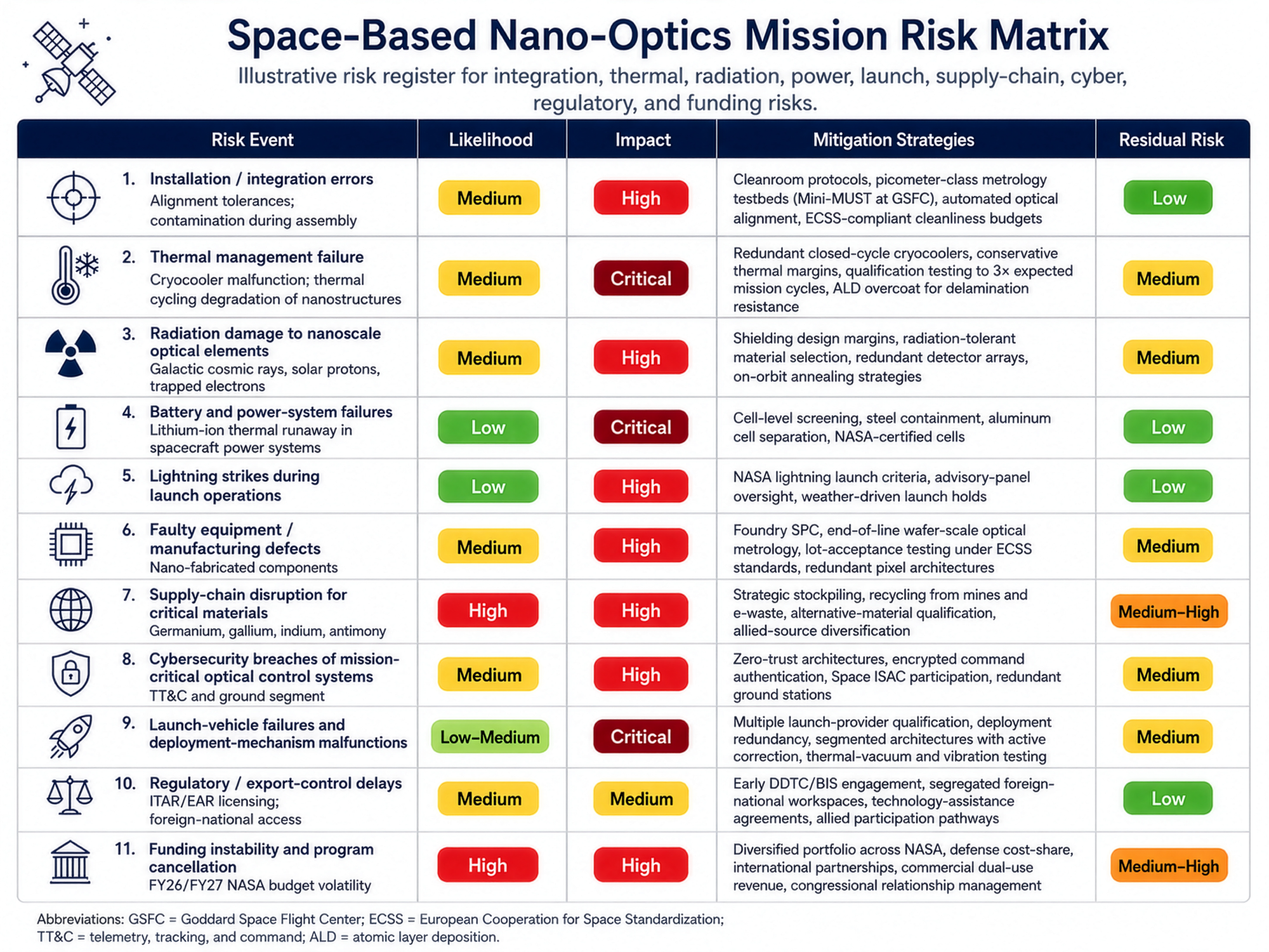
The two highest residual risks: supply-chain disruption and funding instability, are correlated, since rising material costs directly pressure program budgets, and both are heavily exogenous to mission management. The risk matrix should be re-evaluated annually as a minimum, and after any major event (e.g., a new round of Chinese export controls, a continuing-resolution funding gap, or a launch failure affecting access to space).
9. Strategic Recommendations
The recommendations below are tailored to three audience groups. They are staged in order of priority and time horizon, with explicit benchmarks that would alter the recommendation if breached.
9.1 For Policymakers and Government Agencies
Priority 1: Stabilize and expand mid-TRL technology maturation funding. The Strategic Astrophysics Technology program has demonstrated ~100 successful TRL advancement projects at modest cost since 2009 [18]. Congress should treat SAT, APRA, and HWO GOMAP as core infrastructure rather than discretionary research, with multi-year authorization and a floor of $200 million annually (combined) for nanophotonic IR optics maturation. Benchmark: if APRA falls below $80 million in any fiscal year, the U.S. astronomy nanophotonics pipeline should be considered at acute risk.
Priority 2: Modernize export control treatment of dual-use metasurfaces. The current ECCN 0A919 framework, designed for legacy IR FPAs, treats metasurface optics under inconsistent classifications [3]. The Bureau of Industry and Security and the Directorate of Defense Trade Controls should issue a clarifying interpretive rule by FY2027 distinguishing astronomy-grade metasurface optics from ISR/missile-defense applications, reducing licensing friction with Five Eyes and EU partners while preserving controls against PRC and proscribed-destination access. Benchmark: licensing turnaround times for academic and allied-industry metasurface technology should fall below 60 days.
Priority 3: Diversify the germanium and gallium supply chain. Project Vault and similar mineral reserves are necessary but insufficient. The Department of Energy, Department of Defense, and Department of Commerce should jointly fund (a) recovery of germanium and gallium from active and legacy mine waste; (b) e-waste recycling pathways; and (c) qualification of silicon-on-CaF₂ and chalcogenide-glass alternatives for IR optics where performance permits [13][59][60]. Benchmark: U.S. and allied germanium production capacity should reach 30% of consumption by 2030.
Priority 4: Deepen Five Eyes and AUKUS Pillar II cooperation on space-based IR sensing. Existing 5-Eyes ISTAR working groups and SSA collaborations should be expanded to formally include nanophotonic IR optics technology, with shared TRL advancement testbeds and reciprocal foundry access [66][67][68]. Benchmark: at least three jointly funded TRL 5+ demonstrations with allied partners by 2028
Priority 5: Workforce development. The pipeline of U.S. nanophotonics PhDs is heavily reliant on foreign-national talent, much of which faces increasing visa friction. The National Science Foundation, NASA, and the Department of Defense should fund targeted graduate fellowships (~500 per year, ~$50,000 stipend plus tuition) tied to U.S. citizenship or permanent residency, while maintaining open scientific exchange with allied nations.
9.2 For Institutional Investors and Industry Executives
Priority 1: Allocate to dual-use platforms, not pure-play astronomy. The economically viable strategy in nanophotonic IR optics is to build a single technology platform with multiple revenue streams across consumer biometrics, defense ISR, and astronomy. Metalenz’s trajectory; from Harvard IP through DARPA EXTREME funding to STMicroelectronics consumer-electronics partnership and now UMC mass production, exemplifies this pattern [16][40][43]. Benchmark: target portfolios in nanophotonic IR should derive >40% of revenue from non-defense commercial markets within 5 years of investment.
Priority 2: Position around foundry partnerships, not vertical integration. The capital intensity of building dedicated nanophotonic IR fabrication capacity is prohibitive for most participants; the winning model is fabless design with foundry partnerships (UMC, STMicroelectronics, GlobalFoundries, TowerSemiconductor) [16][43]. Benchmark: avoid investments in pure-play designers without secured foundry capacity.
Priority 3: Evaluate IP defensibility carefully. The metasurface patent landscape now exceeds 150 applications and issued patents from Metalenz alone, plus parallel portfolios from Tunoptix, JPL/Caltech, and Chinese institutions. Investors should commission independent freedom-to-operate analyses and weight the value of foundational claims (Capasso Lab portfolio) above incremental design patents [40]
Priority 4: Hedge supply-chain risk explicitly. Companies dependent on germanium-, gallium-, indium-, or antimony-bearing components should maintain at least 12 months of strategic inventory, qualified second-source suppliers from non-Chinese jurisdictions, and active programs for material substitution. Benchmark: target portfolios should pass a stress test assuming 24 months of full Chinese export ban.
Priority 5: Engage with ITAR/EAR exposure at investment time. Every nanophotonic IR investment should include explicit ITAR/EAR diligence, foreign-national workforce policies, and CFIUS-sensitivity assessment. This is particularly material for cross-border deals and for companies serving both NASA and Department of War markets.
9.3 For Research Institutions
Priority 1: Concentrate on the TRL 3–6 mid-gap with credible mission infusion paths. The single most valuable contribution academic groups can make is rigorous environmental qualification of nanophotonic IR optics, cryogenic cycling, radiation, vibration, contamination, at TRL 5/6 against specific mission infusion targets (HWO, PRIMA, future Probes) [18][27].
Priority 2: Pursue collaboration models that align with mission pull. The most successful TRL-advancement patterns involve PI-led teams with PI from a research university, co-investigators at JPL or NASA centers, and at least one industrial partner with foundry access. Benchmark: any nanophotonic IR project not aligned to an explicit mission infusion target by TRL 4 is at risk of stalling.
Priority 3: Prioritize three research directions. First, achromatic broadband metalenses for the 1–5 µm range relevant to HWO biosignature spectroscopy [26]. Second, large format (≥1024 × 1024) photon-counting MWIR/LWIR detectors with sensitivities sufficient for PRIMA-class far-IR spectroscopy [28][29]. Third, radiation-tolerant ALD coatings and metasurface architectures with documented stability through ≥10 krad total ionizing dose [37][38][49].
Priority 4: Engage the policy and standards process. Astronomy nanophotonics will be shaped as much by export-control rules and foundry access as by laboratory innovation. Research institutions should formally engage with NASA’s HWO architecture committees, ESA’s Voyage 2050 working groups, Five Eyes S&T forums, and SPIE/Optica standards committees.
10. Caveats and Confidence Calibration
Several findings in this report rest on data of variable quality. First, market-size estimates for nanophotonics vary by a factor of three across reputable analysts (from ~$16 billion to ~$42 billion in 2024), reflecting definitional disagreement; readers should treat any single point estimate with skepticism [12][51][74]. Second, performance benchmarks for metalenses are typically reported in narrow spectral bands and at small apertures; extrapolation to flagship-aperture astronomy missions involves substantial engineering uncertainty. Third, the FY2027 budget environment for NASA Astrophysics is highly volatile; the President’s Budget Request and final appropriations have diverged by 30% or more in recent cycles, creating planning instability that could materially affect the timelines discussed [54][55]. Fourth, claims about Chinese photonics performance (e.g., the Tsinghua “ACCEL” chip’s reported 3,000× speed advantage) are contested and were sourced from CSIS commentary; they should be treated as preliminary [58]. Fifth, radiation tolerance data for metasurfaces in the L2 environment is sparse, and most published radiation studies have used 2D-material or solar-cell test articles rather than full metalens architectures [49][50]. Sixth, this report does not address the classified portions of national-security IR sensing, which materially shape the technology base but cannot be analyzed in open-source format.
The author’s confidence is highest in the technology-base findings (Sections 2 and 4), in the regulatory mapping (Section 6), and in the supply-chain analysis (Section 5.6); medium in the market-sizing and venture-capital analysis (Section 5); and lowest in specific performance projections for missions still in pre-Phase A (Section 2.1).
References
[1] Aerospace Corporation. (n.d.). Novel satellite deorbiting method can help mitigate orbital debris. The Aerospace Corporation. https://aerospace.org/
[2] American Astronomical Society. (2025, May 30). The FY26 President's Budget Request: NASA and NSF details. AAS. https://aas.org/posts/news/2025/06/fy26-presidents-budget-request
[3] American Astronomical Society. (2026a, January 16). Congress passes fiscal year 2026 spending bills for NSF, NASA, and DOE. AAS. https://aas.org/posts/news/2026/01/
[4] American Astronomical Society. (2026b, April). The FY27 President's Budget Request: NASA, NSF, and DOE details. AAS. https://aas.org/posts/news/2026/04/fy27-presidents-budget-request-nasa-nsf-and-doe-details
[5] AmeriCOM. (2025, May 22). Strain on our germanium supply chain: A shortage we can't afford to ignore. AmeriCOM. https://americom.org/2025/05/22/
[6] Bureau of Industry and Security. (2017, January 13). Increase of controls: Infrared detection items. Federal Register.
[7] Capasso, F., et al. (2018). Solid-immersion metalenses for infrared focal plane arrays. arXiv:1805.06608.
[8] Center for Strategic and International Studies (Allen, G. C., et al.). (2024). Controlling light: Is silicon photonics an emerging front in U.S.-China tech competition? CSIS.
[9] Center for Strategic and International Studies (Swope, C.). (2025). Strategic trajectories: Assessing China's space rise and the risks to U.S. leadership [Congressional testimony]. CSIS.
[10] Centre for International Governance Innovation. (2022). The Five Eyes and space: A new frontier for an old intelligence alliance. CIGI Articles.
[11] Chandrasekar, R. (2023). Overview of DARPA programs transitioning metasurfaces to imaging applications. Proceedings of SPIE PC12514, PC1251401.
[12] DARPA. (2021). DARPA, NGA transition novel optics technology to fieldable prototypes [Press release]. Defense Advanced Research Projects Agency.
[13] Dalton, P. J., & North, T. (2018). International Space Station lithium-ion main battery thermal runaway propagation test (NTRS-20180000927). NASA Technical Reports Server.
[14] European Cooperation for Space Standardization. (2008). ECSS-Q-ST-70-06C: Particle and UV radiation testing for space materials.
[15] Federal Register. (2017, January 13). Increase of controls: Infrared detection items.
[16] FTI Consulting. (2024). China's export controls on critical minerals: Gallium, germanium, graphite. FTI Insights.
[17] Gardner, J. P., et al. (2023). The James Webb Space Telescope mission: Optical telescope element design, development, and performance. arXiv:2301.01779.
[18] Glenn, J., et al. (2025). PRIMA mission concept. Journal of Astronomical Telescopes, Instruments, and Systems, 11(3), 031628.
[19] Hennessy, J., et al. (2024). Atomic layer processing coating techniques enable missions to see further into the ultraviolet. NASA Science Technology Highlight. NASA.
[20] IMARC Group. (2025). Nanophotonics market size, share and forecast to 2033. IMARC Group.
[21] Jet Propulsion Laboratory. (n.d.). Atomic layer deposition (ALD) for detector, optics, and filters fabrication and enhancement. NASA JPL Microdevices Laboratory.
[22] Knobbe Martens. (2025). Space technology investments clear the launch tower in 2025. Knobbe Martens Aerospace Blog.
[23] Krider, E. P., et al. (1970). Analysis of Apollo 12 lightning incident. NASA Technical Report.
[24] Laser Focus World. (2024). Germanium and gallium supply chain disruption escalates for U.S. Laser Focus World.
[25] Leonardo DRS. (2024). Cooled infrared technology. Leonardo DRS Product Documentation.
[26] Magnolia Optical Technologies / Sood, A. K., Zeller, J. W., et al. (2021). Development of nanostructured antireflection coating technology for IR band for improved detector performance. Proceedings of SPIE, 11858, 1185812.
[27] MarketsandMarkets. (2025). Photonics market by product, wavelength, material, application, and end-use industry — global forecast to 2030. MarketsandMarkets.
[28] Metalenz, Inc. (2025, August 18). Metalenz expands its technologies in the metasurface market to include system level sensing applications. GlobeNewswire.
[29] Military Aerospace. (2024). The next frontier of electro-optical sensors. Military Aerospace.
[30] Moullet, A., et al. (2023). PRIMA general observer science book. arXiv:2310.20572.
[31] Nagler, P. C., Sadleir, J. E., & Wollack, E. J. (2020). Transition-edge sensor detectors for the Origins Space Telescope. arXiv:2012.06549.
[32] National Academies of Sciences, Engineering, and Medicine. (2021). Pathways to discovery in astronomy and astrophysics for the 2020s. National Academies Press.
[33] National Aeronautics and Space Administration. (2024). FY 2025 budget request agency summary. NASA Office of the Chief Financial Officer.
[34] National Aeronautics and Space Administration. (2024, October 3). NASA selects AXIS and PRIMA for studies. NASA Science.
[35] National Aeronautics and Space Administration. (2025). Habitable Worlds Observatory. NASA Science.
[36] NIST National Cybersecurity Center of Excellence. (2024). Cybersecurity for the space domain. NCCoE.
[37] Open Research Foundation – America. (2024). China's critical mineral export controls: Background and chokepoints. ORF America.
[38] Optics & Photonics News. (2011). Optical innovations in the James Webb Space Telescope. Optica Publishing, 22(11).
[39] Park, J.-S., et al. (2024). All-glass 100 mm diameter visible metalens for imaging the cosmos. ACS Nano, 18.
[40] Planetary Society. (2025). NASA's FY 2025 budget. The Planetary Society.
[41] Rieke, G. H., et al. (2015). The mid-infrared instrument for the James Webb Space Telescope, VII: The MIRI detectors. arXiv:1508.02362.
[42] Siegmund, W. A., & Roellig, T. (2018). Origins Space Telescope: The far infrared imager and polarimeter FIP. 231st AAS Meeting Abstract.
[43] Siler, S. (2024). How NASA has made lithium-ion batteries safer for spacecraft. Battery Technology Online.
[44] Soifer, B. T., Werner, M. W., & Lawrence, C. (2004). The Spitzer Space Telescope mission. arXiv:astro-ph/0406223.
[45] Sood, A. K., et al. (2022). Nanostructured antireflection coating technology for enhanced MWIR and LWIR band sensing performance. Proceedings of SPIE, 12234, 1223412.
[46] Space Telescope Science Institute. (2025). JWST optics. STScI Documentation.
[47] Space Telescope Science Institute. (2025). Towards the Habitable Worlds Observatory: Visionary science and transformational technology. STScI Workshop Proceedings.
[48] Stahler, T. J., et al. (2018). Composite reflective/absorptive IR-blocking filters embedded in metamaterial antireflection coated silicon. arXiv:1702.08454.
[49] Tunoptix / University of Washington Nanofabrication Facility. (2020). Optics startup Tunoptix wins federal grant to develop metalenses for imaging satellites at WNF. UW WNF News.
[50] U.S. Geological Survey. (2024). Mineral commodity summaries 2024: Germanium and gallium. USGS.
[51] U.S. International Trade Commission. (2023). Germanium and gallium: U.S. trade and Chinese export controls. USITC Executive Briefing on Trade.
[52] Werner, M. (2005). A short and personal history of the Spitzer Space Telescope. arXiv:astro-ph/0503624.
[53] Zhang, F., et al. (2025). Centimeter-size achromatic metalens in long-wave infrared. Nanophotonics, 14(3), 421–435. https://doi.org/10.1515/nanoph-2024-0716
[54] Zhang, L., et al. (2022). High-efficiency, 80-mm aperture metalens telescope. Nano Letters, 22(24), 10058–10064.
[55] Zhao, Y., et al. (2024). Theoretical performance limitations and filter selection based on Fisher information of a computational photonic crystal spectrometer for trace-gas retrieval. arXiv:2411.02048.